

TI公司的ADS5263是采用CMOS工艺技术的具有低噪音16位前端和14位ADC的低功耗非常高SNR性能的集成电路,SNR可达85dBFS(10MHz),30MHz时可达80dBFS,最大取样速率00 MSPS,可编程增益0 dB 到12 dB,主要用在医疗成像如MRI, 波谱学和CCD图像.本文介绍了ADS5263主要特性,方框图, 数字处理框图以及ADS5263EVM评估板电路图,材料清单和元件布局图.
Using CMOS process technology and innovative circuit techniques, the ADS5263 is designed to operate at low power and give very high SNR performance with a 4-Vpp full-scale input. Using a low-noise 16-bit front-end stage followed by a 14-bit ADC, the device gives 85-dBFS SNR up to 10 MHz and better than 80-dBFS SNR up to 30 MHz.
The device also has a 14-bit low power mode, where it operates as a quad-channel 14-bit ADC. The 16-bit front-end stage is powered down and the part consumes almost half the power, compared to the 16-bit mode. The 14-bit mode supports a 2-Vpp full-scale input signal, with typical 74-dBFS SNR. The ADS5263 can be dynamically switched between the two resolution modes. This allows systems to use the same part in a high-resolution, high-power mode or a low-resolution, low-power mode.
ADS5263主要特性:
Maximum Sample Rate: 100 MSPS
Programmable Device Resolution
Quad-Channel, 16-Bit, High-SNR Mode
Quad-Channel, 14-Bit, Low-Power Mode
16-Bit High-SNR Mode
1.35 W Total Power at 100 MSPS338 mW/Channel
4 Vpp Full-scale Input
85-dBFS SNR at fin = 3 MHz, 100 MSPS
14-Bit Low-Power Mode
785 mW Total Power at 100 MSPS195 mW/Channel
2-Vpp Full-Scale Input
74-dBFS SNR at fin = 10 MHz
Integrated Clamp (for interfacing to CCD sensors)
Low-Frequency Noise Suppression
Digital Processing Block
Programmable FIR Decimation Filters
Programmable Digital Gain: 0 dB to 12 dB
2- or 4-Channel Averaging
Programmable Mapping Between ADC Input Channels and
LVDS Output Pins—Eases Board Design
Variety of Test Patterns to Verify Data Capture by FPGA/Receiver
ADS5263应用:
• Medical Imaging – MRI
• Spectroscopy
• CCD Imaging
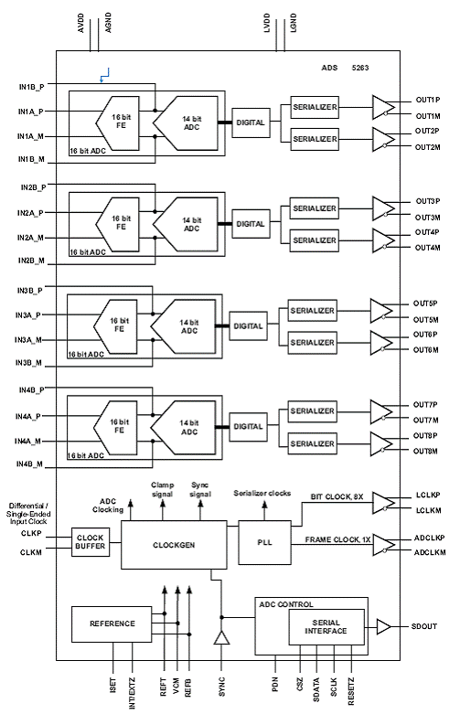
图1.ADS5263功能方框图
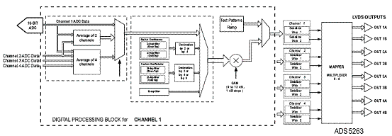
图2.ADS5263数字处理框图
ADS5263EVM评估板
This user’s guide gives an overview of the ADS5263EVM and describes how the evaluation module can be used to evaluate the performance, functions, and features of the ADS5263 device.
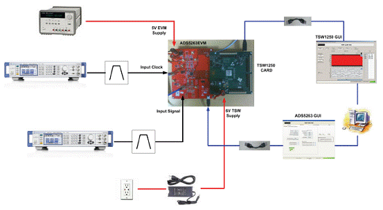
图3.ADS5263EVM评估板建立框图
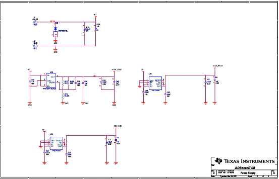
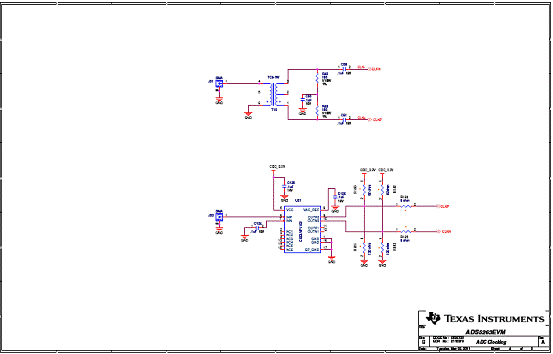
图4.ADS5263EVM评估板电路图(1)
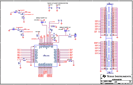
图5.ADS5263EVM评估板电路图(2)
